MSc thesis project proposal
Sub-mm Printing Process Evaluation of Copper Sinter Paste for Copper Pillars on All-Printed SMD Components
Project outside the university
CITCThere is industrial interest to reducethe costs of current manufacturing process for printed surface-mount devices (SMD). Resistive elements can be printed, but bumping remains challenging. Replacing expensive metallization processes with printed copper pillars can potentially reduce product costs, processing steps, and facilitate flip-chip bonding. Copper sintered pillars favours soldering unlike Silver which suffers from diffusion of solders.
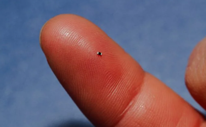
Nearly the smallest chip resistor package, 0402, has a footprint of 1mm x 0.5mm. The printable area on such small footprint would be in sub-mm range (tentatively 0.2mm x 0.4mm). Various SMD resistor sizes exist, with the smallest chip resistor package, 0201, which requires printing over an area of < 0.2mm x 0.2mm tentatively.
The following opportunities and challenges set the background for this project:
- Conventional screen printers lack the necessary resolution to reach sub-mm printing.
- A high-aspect ratio of at last 1 is required.
- Strong adhesion to the substrate
- A target bump thickness of 20 to 30 um
Assignment
Investigate different processes for printing different sizes of copper pillars that are compatible with various SMD codes. The expected project flow is as follows:
- Material scouting – Explore potential printable copper pastes and their curing processes (pressure/pressureless)
- Material testing – Conduct some preliminary material tests to evaluate the bond strength to Ag.
- Printing process analysis – Evaluate screen/stencil printing resolution limitation using DEK printer at TNO/CITC and further explore photolithographic stencil printing at EKL [2].
- Prototype printing – Demonstrate successful printing over a large substrate with SMD components.
- Explore the advantages and drawbacks with comparison to other processes.
- Final presentation internally at CITC and Master thesis defence at TU Delft.
Note: The process of thesis writing goes hand-in-hand throughout the process flow.
Requirements
- Location – Flexible (EKL Delft / CITC Nijmegen)
- Collaborators – CITC and TU Delft
- Duration – 6 to 8 months.
- Requirements – Current MSc students from Mechanical / Electrical Engineering
- Supervisors – Henry Antony Martin (CITC), Edsger Smits (CITC), and Henk van Zeijl (TU Delft)
- Internship Stipend – Standard internship stipend provided by CITC. Travel allowance can be discussed.
Contact
dr. Massimo Mastrangeli
Electronic Components, Technology and Materials Group
Department of Microelectronics
Last modified: 2025-02-17